Gan On Sapphire Strain

A Hrtem Image Of The Gan Sapphire Interface In The Gan Film On The Download Scientific Diagram

A Hrtem Image Of The Gan Sapphire Interface In The Gan Layer On The Download Scientific Diagram

Comparison Of Strain Relaxation Of Gan On Aln Sapphire And Aln Single Download Scientific Diagram

Critical Thickness Of Gan Film In Controllable Stress Induced Self Separation For Preparing Native Gan Substrates Sciencedirect

Nanotechnology Energy Generation Using Sound In 2020 Nanotechnology Science And Technology Innovative Research

Xrd Scans Of Aln Grown On The Sapphire 0001 On Axis Substrates With Download Scientific Diagram

An enhanced strain relaxation was observed in gan grown on a stack of five ingan layers each 200 nm thick with the in content increased in each layer and with an intermediate thin gan layer 10 nm thick inserted between the ingan layers as compared.
Gan on sapphire strain.

Strain Relaxation In Ingan Gan Multiple Quantum Wells By Nano Patterned Sapphire Substrates With Smaller Period Semantic Scholar

Thermal Profile Of Gan Hemts On A Silicon And B Sapphire Substrates Download Scientific Diagram

Analysis Of The Interface Structure Of Aln On Sapphire Theoretically Download Scientific Diagram

Pdf Stress And Wafer Bending Of A Plane Gan Layers On R Plane Sapphire Substrates

Defect Analysis Of The Led Structure Deposited On The Sapphire Substrate Sciencedirect
New Page 1

Growth Of High Quality Gan On A Novel Designed Bonding Thinned Template By Hvpe Crystengcomm Rsc Publishing Doi 10 1039 C2ce25363a
High Quality Aln Epilayers Grown On Nitrided Sapphire By Metal Organic Chemical Vapor Deposition Scientific Reports

Schematic Diagram Of Led Structures With An In Situ Lt Gan Nucleation Download Scientific Diagram
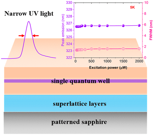
Near Strain Free Gan Algan Narrow Line Width Uv Light Emission With Very Stable Wavelength On Excitation Power By Using Superlattices Acs Appl Electron Mater X Mol
Facile Au Assisted Epitaxy Of Nearly Strain Free Gan Films On Sapphire Substrates Rsc Advances Rsc Publishing Doi 10 1039 C9ra09689b

Sapphire Nanomembrane Technology For High Efficiency Micro Led Displays Conference Presentation

Ultralow Threading Dislocation Density In Gan Epilayer On Near Strain Free Gan Compliant Buffer Layer And Its Applications In Hetero Epitaxial Leds Abstract Europe Pmc

Direct Van Der Waals Epitaxy Of Stress Free Gan Films On Pecvd Grown Graphene Sciencedirect
Https Www Mdpi Com 2076 3417 9 4 788 Pdf
Https Www Nature Com Articles S41598 020 69946 4 Pdf Origin Ppub

Barrier Strain And Carbon Incorporation Engineered Performance Improvements For Algan Gan High Electron Mobility Transistors Luong 2015 Chemical Vapor Deposition Wiley Online Library

Rheed Pattern Of A Initial Aln Sapphire And B Aln Aln Single Download Scientific Diagram

Movpe Growth Of Aln Films On Nano Patterned Sapphire Substrates With Annealed Sputtered Aln Sciencedirect

Microstructure Variation In Thick Alinn Films Grown On C Plane Gan On Sapphire By Metalorganic Chemical Vapor Deposition Sciencedirect
Vertical Gallium Nitride Light Emitting Diodes On 4 Inch Silicon Wafers

Lattice Strain In Bulk Gan Epilayers Grown On Crn Sapphire Template Applied Physics Letters Vol 94 No 8

W Rocking Curves Of The 0002 Gan On Sapphire Wafer B Before Download Scientific Diagram

A Multilevel Intermediate Band Solar Cell By Ingan Gan Quantum Dots With A Strain Modulated Structure Sang 2014 Advanced Materials Wiley Online Library

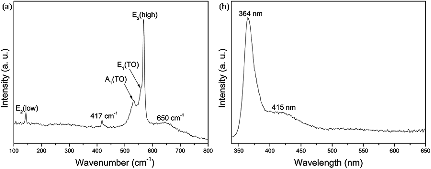
Pdf Raman Studies Of Gan Sapphire Thin Film Heterostructures

Figure 1 From Bow Of Hvpe Wafers 25 Wafer Bow Of Freestanding Gan Substrates Grown By Hydride Vapor Phase Epitaxy Semantic Scholar

Pdf Growth Of A Plane Zno Thin Films On R Plane Sapphire By Plasma Assisted Mbe
Pdf High Resolution X Ray Diffraction Strain Stress Analysis Of Gan Sapphire Heterostructures
Https Www Osapublishing Org Copp Viewmedia Cfm Uri Copp 1 4 358 Seq 0
Facile Au Assisted Epitaxy Of Nearly Strain Free Gan Films On Sapphire Substrates Rsc Advances Rsc Publishing
Https Ieeexplore Ieee Org Iel7 8652085 8656628 08657271 Pdf

4 Inch N Type Undoped 4 Um Gan Epitaxial Template On Sapphire 0001 Mse Supplies Llc
Analysis Of Doping Induced Wafer Bow During Gan Si Growth On Sapphire Journal Of Applied Physics Vol 112 No 3
Gan Leds On Si Substrate Springerlink

Dependence Of Offset Voltage In Algan Gan Van Der Pauw Devices Under Mechanical Strain Sciencedirect

Kith Blue Label Essex Jacket Tahiti Apparel Kith Nyc His Style Tropical Fashion Fashion M65 Jacket

Crack Free Gan Based Ultraviolet Multiple Quantum Wells Structures Grown On Aln 2 Misoriented Sapphire Template Sciencedirect

A Xps Spectral Surveys Of The Nearly Strain Free Gan Films Xps Download Scientific Diagram

Pdf Growth Defects In Gan Films On Sapphire The Probable Origin Of Threading Dislocations
Https Onlinelibrary Wiley Com Doi Pdf 10 1002 Pssa 201700323

Stress And Wafer Bending Of A Plane Gan Layers On R Plane Sapphire Substrates Journal Of Applied Physics Vol 100 No 10
Https Ieeexplore Ieee Org Iel7 3 6671407 06674047 Pdf

Selective Heteroepitaxy On Deeply Grooved Substrate A Route To Low Cost Semipolar Gan Platforms Of Bulk Quality Applied Physics Letters Vol 109 No 8

Pdf High Thermal Conductivity Of Gallium Nitride Gan Crystals Grown By Hvpe Process
Source : pinterest.com
