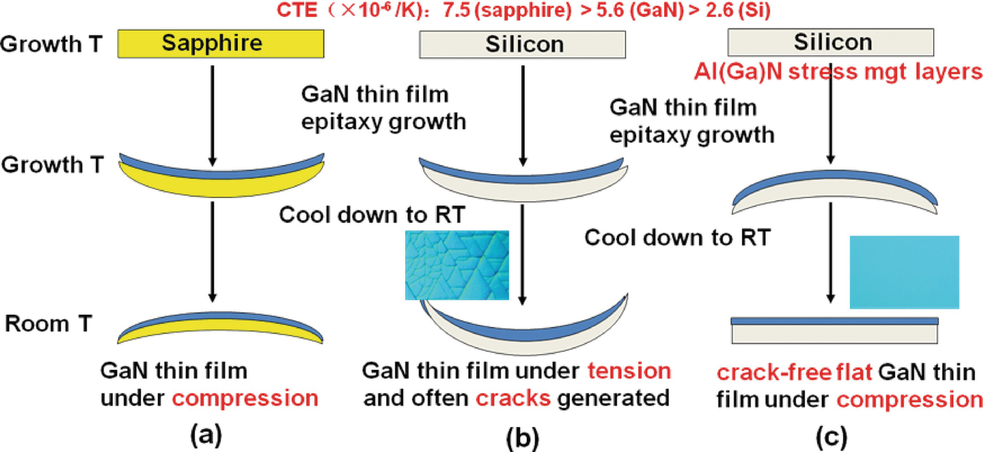
Gan On Sapphire Stress

Critical Thickness Of Gan Film In Controllable Stress Induced Self Separation For Preparing Native Gan Substrates Sciencedirect

Pdf Thick Gan Film Stress Induced Self Separation

All About Led Lamp Technical Use Substrate Microfabrication Double Led Brightness Substrate Led Doubles

Schematic Diagram Illustrating The Overgrowth Process Of Gan Thick Download Scientific Diagram

Stress Induced In Situ Epitaxial Lateral Overgrowth Of High Quality Gan Crystengcomm Rsc Publishing Doi 10 1039 C4ce01003e

Pdf Characterization Of Stress In Gan On Sapphire Microelectromechanical Systems Mems Structures Using Micro Raman Spectroscopy Semantic Scholar

To vary from 0 gan surface to 5 0 kj mole gan sapphire interface but in the case of h movpe grown samples the strain energy varied from 6 5 kj mole hydrostatic strain gan surface to 25 0 kj mole biaxial strain gan sapphire interface indicating that the surface layer of the n terminated h movpe material is not free from strain.
Gan on sapphire stress.

Foreign Substrate An Overview Sciencedirect Topics

4jgfpfvt0s92xm

A Correlation Between The Wafer Curvature And Residual Mechanical Download Scientific Diagram

Room Temperature Raman Spectra Of Gan Films Grown On Aplane Sapphire Download Scientific Diagram
Https Compoundsemiconductor Net Article 101896 Gan Hemts The Substrate Conundrum Feature
A Raman Spectra Of The Gan Led Structure On A Sapphire Substrate Download Scientific Diagram

Pdf Stress And Its Effect On Optical Properties Of Gan Epilayers Grown On Si 111 6h Sic 0001 And C Plane Sapphire Semantic Scholar
Wafer Scale Fabrication Of Non Polar Mesoporous Gan Distributed Bragg Reflectors Via Electrochemical Porosification Scientific Reports

What Are Heart Rate Monitor Watches Golf Watch Golf Gps Watch Cheap Golf Clubs
Http Iopscience Iop Org Article 10 1088 1361 6641 Aa7248 Pdf
Https Iopscience Iop Org Article 10 1149 2162 8777 Aba7fc Pdf

Pdf Characterization Of Gan Grown On 4h Sic And Sapphire By Raman Spectroscopy And High Resolution Xrd Semantic Scholar

Impact Of Cone Shape Patterned Sapphire Substrate And Temperature On The Epitaxial Growth Of P Gan Via Mocvd Yao 2019 Physica Status Solidi A Wiley Online Library

Residual Stress Of Curvature Sapphire Substrate With Gan Film Released By The Application Of Trench Structures Semantic Scholar

Investigation Of Nitridation Time On The Quality Of Algan Gan Heterojunction Grown On Aln Sputtered Sapphire Substrate Sciencedirect

Nanotechnology Energy Generation Using Sound In 2020 Nanotechnology Science And Technology Innovative Research

Pin By Mila Zamora On Fur Love Calm Dogs Natural Dog Calming Oils

Incorporation Of Air Cavity Into Sapphire Substrate And Its Effect On Gan Growth And Optical Properties Sciencedirect
Non Polar Gallium Nitride Ultraviolet Photodetector On Sapphire

Lima Blue Rug Rug Design Blue Kilim Blue Rug

Gan On Si Epitaxy Dadgar Major Reference Works Wiley Online Library

Direct Van Der Waals Epitaxy Of Stress Free Gan Films On Pecvd Grown Graphene Sciencedirect

Rustic Chic Geo Rug Chic Rug Modern Kilim Black Area Rugs
Crystals Special Issue Gan Based Optoelectronic Materials And Light Emitting Devices

Growth Of High Quality Gan On A Novel Designed Bonding Thinned Template By Hvpe Crystengcomm Rsc Publishing Doi 10 1039 C2ce25363a

Representative Raman Spectra Showing The Shift In Energy Of The E 2 2 Download Scientific Diagram

Role Of Growth Temperature On Formation Of Single Crystalline Gan Nanorods On Flexible Titanium Foil By Laser Molecular Beam Epitaxy Sciencedirect
Https Www Osapublishing Org Ome Viewmedia Cfm Uri Ome 9 4 1945 Seq 0

Fabrication Of Non Polar Gan Based Highly Responsive And Fast Uv Photodetector Applied Physics Letters Vol 110 No 10

Mechanisms In Thermal Stress Aided Electroless Etching Of Gan Grown On Sapphire And Approaches To Vertical Devices Rsc Advances Rsc Publishing Doi 10 1039 C3ra40794b
Gan Leds On Si Substrate Springerlink

Pdf Raman Studies Of Gan Sapphire Thin Film Heterostructures

Expanding The Application Potential Of Hydride Vapor Phase Epitaxy

Laser Molecular Beam Epitaxy Growth Of Porous Gan Nanocolumn And Nanowall Network On Sapphire 0001 For High Responsivity Ultraviolet Photodetectors Sciencedirect

Effects Of Carrier Gas On The Stress Of A Plane Gan Films Grown On R Plane Sapphire Substrates By Metalorganic Chemical Vapor Deposition Sciencedirect
Mechanism Of Stress Driven Composition Evolution During Hetero Epitaxy In A Ternary Algan System Scientific Reports

Blue And White Chinoiserie Decor Items For Weddings And Events Chinoiserie Wedding Blue White Weddings Ginger Jars Wedding

Simple Love Opening Bracelet Silver Gold Rose Gold Cuff Bangle Bracelets Gift For Women Dia Simple Silver Jewelry Jewelry Women Gold Silver Bracelets For Women
Cross Stacked Carbon Nanotubes Assisted Self Separation Of Free Standing Gan Substrates By Hydride Vapor Phase Epitaxy Scientific Reports

Pdf Recent Progress Of High Quality Gan Substrates By Hvpe Method
A Bow Free Freestanding Gan Wafer Rsc Advances Rsc Publishing Doi 10 1039 D0ra01024c

Gan In Different Dimensionalities Properties Synthesis And Applications Sciencedirect

Thousand Dollar Mushroom From The Kingdom Of Bhutan Stuffed Mushrooms Thousand Dollars Bhutan

Freestanding Gan Substrate Enabled By Dual Stack Multilayer Graphene Via Hydride Vapor Phase Epitaxy Sciencedirect
Source : pinterest.com
